- English
- French
- German
- Portuguese
- Spanish
- Russian
- Japanese
- Korean
- Arabic
- Greek
- German
- Turkish
- Italian
- Danish
- Romanian
- Indonesian
- Czech
- Afrikaans
- Swedish
- Polish
- Basque
- Catalan
- Esperanto
- Hindi
- Lao
- Albanian
- Amharic
- Armenian
- Azerbaijani
- Belarusian
- Bengali
- Bosnian
- Bulgarian
- Cebuano
- Chichewa
- Corsican
- Croatian
- Dutch
- Estonian
- Filipino
- Finnish
- Frisian
- Galician
- Georgian
- Gujarati
- Haitian
- Hausa
- Hawaiian
- Hebrew
- Hmong
- Hungarian
- Icelandic
- Igbo
- Javanese
- Kannada
- Kazakh
- Khmer
- Kurdish
- Kyrgyz
- Latin
- Latvian
- Lithuanian
- Luxembou..
- Macedonian
- Malagasy
- Malay
- Malayalam
- Maltese
- Maori
- Marathi
- Mongolian
- Burmese
- Nepali
- Norwegian
- Pashto
- Persian
- Punjabi
- Serbian
- Sesotho
- Sinhala
- Slovak
- Slovenian
- Somali
- Samoan
- Scots Gaelic
- Shona
- Sindhi
- Sundanese
- Swahili
- Tajik
- Tamil
- Telugu
- Thai
- Ukrainian
- Urdu
- Uzbek
- Vietnamese
- Welsh
- Xhosa
- Yiddish
- Yoruba
- Zulu
Technological Innovation
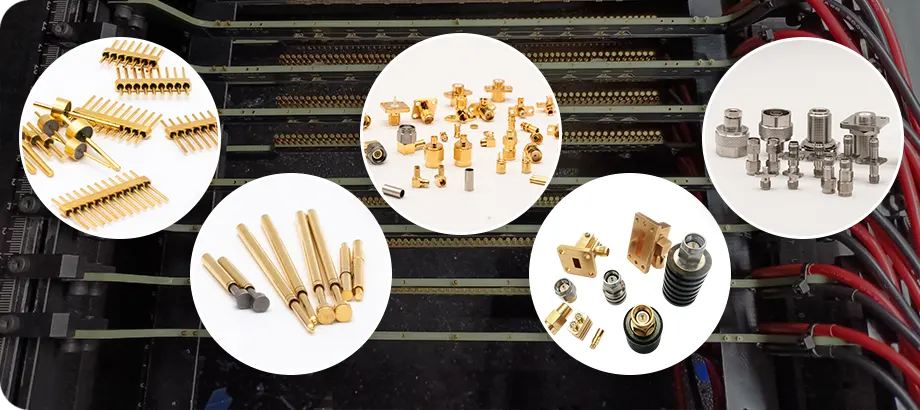
Shaanxi Chuangyu Core Innovation Technology System
With nearly two decades of technical expertise in precision electronics from its core team, Chuangyu Electronics pursues its mission to "break through technological barriers and address industry pain points." The company has established an innovative technological framework in two key sectors—radio frequency communication and semiconductor and photovoltaic testing—focusing on three core areas: high-frequency transmission, precision testing, and integrated interconnectivity. Its technological breakthroughs have not only broken foreign monopolies and filled domestic gaps but also enhanced product competitiveness while driving technological upgrades across related industries, serving as the core engine for the company's rapid growth.
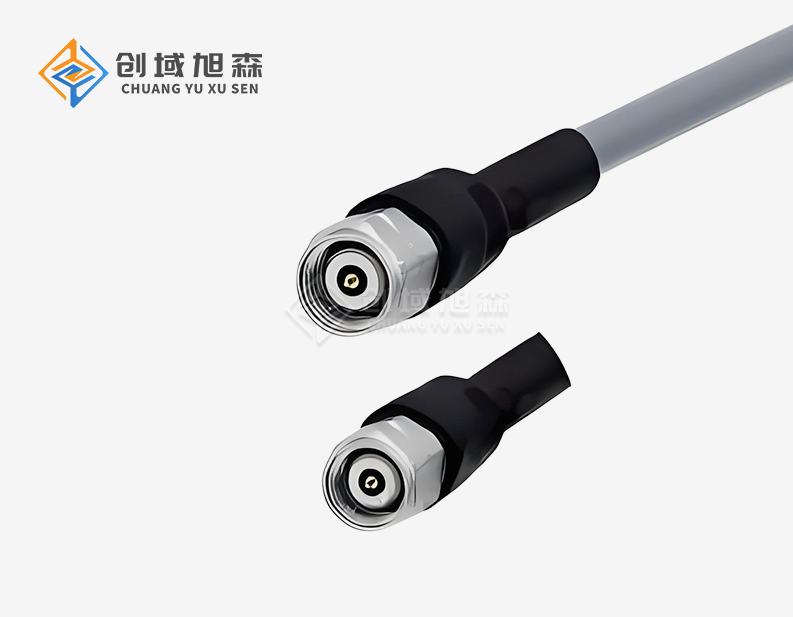
Innovation in RF Communication:Overcoming Transmission Challenges in High Frequency and Special Environment
To address the core demands of RF communication development towards "higher frequency, smaller size, and better environmental adaptability," the company has focused on controlling high-frequency signal transmission loss, designing precision structures, and developing specialized processes. These efforts have resulted in three core innovative technologies tailored for high-end applications such as 5G communications, aerospace, and advanced testing instruments.

145GHz High Frequency RF Connection Technology
This technology represents the company's core achievement in high-end high-frequency communication, overcoming three key technical challenges: miniaturized structural design, signal loss control, and precision machining. It has been successfully implemented in 0.8mm high-frequency RF connectors, achieving stable signal transmission at 145GHz with performance reaching industry-leading standards.
- Technical breakthrough: The "gradient impedance matching structure" design optimizes the dimensional accuracy of inner and outer conductors through 3D electromagnetic field simulation, controlling impedance error within 50Ω±1Ω to effectively reduce high-frequency signal transmission loss. The insertion loss is ≤0.3dB/100mm at 145GHz. An innovative micron-level precision turning process achieves ±0.005mm tolerance control for the 0.8mm ultra-compact connector, ensuring connection stability and repeatability.
- Practical Value: This breakthrough has shattered foreign brands 'monopoly in high-frequency connectors above 100GHz, solving the critical shortage of core components for China's high-end millimeter-wave radar and satellite communication systems. The product is now mass-produced for leading domestic telecom equipment manufacturers, accelerating the localization of high-end RF communication equipment.
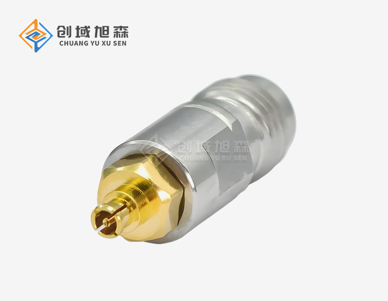
High Vacuum Environment Sealing Penetration Technology
To meet the RF transmission requirements in aerospace and high-vacuum testing equipment, the company has developed a precision sealing technology combining carbide alloy and glass. This innovation is applied to sealed through-penetrating feed insulators, achieving dual functions of "electrical transmission and high-vacuum sealing", thereby filling the technical gap in this field in China.
- Technical breakthrough: The innovative "pre-oxidation-gradient heating sealing" process precisely controls thermal expansion coefficient matching between carbide alloy and glass, effectively resolving interface cracking issues in conventional sealing techniques. This achieves a product air leakage rate of ≤1×10⁻¹⁰ Pa·m³/s, far exceeding industry standards. Simultaneously, the optimized internal conductor structure ensures stable RF signal transmission across a wide temperature range of-55℃ to 125℃, with insulation resistance ≥10¹²Ω.
- Application Value: It provides reliable RF signal transmission solutions for special fields such as spacecraft communication systems and high-vacuum coating equipment. Having passed relevant qualification certifications in the aerospace field, it has become one of the few domestic enterprises with R&D and mass production capabilities for such products.


110GHz Waveguide Coaxial Conversion Technology
To address the challenge of efficient signal conversion between waveguide and coaxial systems, the company has independently developed 110GHz waveguide-to-coaxial conversion technology. This innovation enables seamless low-loss, high-stability transition between the two transmission modes, serving as a critical technical backbone for high-end RF system integration.
- Technical breakthroughs: The design employs a "gradual transition structure" to optimize the impedance matching curve between waveguide and coaxial through simulation, achieving a signal conversion efficiency of ≥98% and a standing wave ratio (SWR) ≤1.2. Additionally, an integrated metal forging process minimizes structural joints, enhancing the product's mechanical strength and signal shielding performance, with an isolation degree (ID) ≥65dB to effectively prevent signal crosstalk.
- Application value: It is widely used in satellite measurement and control, millimeter wave communication and other high-end systems, which solves the problems of high loss and poor stability of traditional conversion equipment, and improves the transmission efficiency and reliability of the whole RF system.
Testing Probe and Module Field Innovation Technology: Achieving Dual Upgrades of Precision and Efficiency
To address the core requirements of 'long lifespan, high density, and high precision' in photovoltaic and semiconductor testing, the company has developed multiple innovative technologies for test probes and integrated modules. These advancements have significantly improved testing efficiency and reliability, establishing the company as a key supplier to leading domestic photovoltaic enterprises.

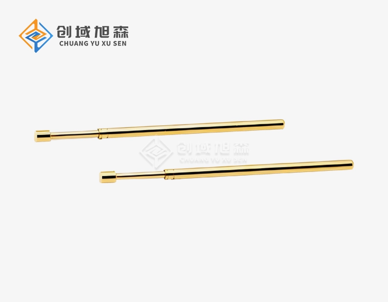
Technology of 5 million times long life photovoltaic EL test probe
To tackle the industry pain point of frequent probe wear and replacement in PV module testing, the company has developed a highly wear-resistant and elastic photovoltaic EL test probe technology, extending the product's service life to 5 million cycles—more than five times the industry average.
- Technical breakthrough: The innovative "tungsten carbide alloy substrate + diamond coating" composite structure achieves a substrate hardness of over HRC65 and a coating hardness of ≥HV2500, significantly enhancing probe wear resistance. Through finite element analysis, the probe's elastic structure is optimized to maintain a consistent tip pressure of 50-80g, preventing cell damage caused by uneven pressure. The design also ensures elastic deformation remains ≤5% after 1 million tests.
- Key benefits: This solution dramatically reduces probe replacement costs and production downtime for photovoltaic manufacturers. For example, a 10GW annual production line can save over 2 million yuan in annual O&M expenses. It has been widely adopted by industry leaders like LONGi and Jinko Solar, establishing itself as the preferred testing solution in photovoltaic manufacturing.
High Density Multi-channel Photovoltaic Testing Module Technology
To address the high-density testing requirements for photovoltaic modules, the company has integrated multi-channel testing technology with signal conditioning technology, developing a multi-channel photovoltaic testing module. This innovation enables a transition from single-channel to multi-channel testing, significantly enhancing testing efficiency.
- Technical breakthrough: The system employs "parallel signal processing + intelligent calibration" technology, enabling a single module to support 3,500 parallel test channels with 5-8 times higher efficiency. Its integrated multi-lead integrated molding technology and high-precision anti-interference circuit effectively resolve signal crosstalk during multi-channel operation, achieving testing accuracy within 0.5%. The rapid fault localization capability significantly reduces maintenance complexity.
- Key Benefits: Designed to meet the high-efficiency testing requirements of photovoltaic module production lines, this solution helps enterprises boost production capacity. Particularly effective for testing large-size, high-density PV modules, it has become the core supporting technology for upgrading photovoltaic testing equipment.


High Precision Test Probe Technology for Semiconductor Chips
To meet the semiconductor chip testing requirements of "high precision and low damage", the company has developed micron-level precision test probe technology, which can adapt to the testing needs of different chip specifications, ensuring the accuracy of test data and the safety of chips.
- Technical breakthrough: The "laser microfabrication" process achieves probe tip precision below 0.5μm, enabling precise alignment with microchip pads. The innovative "flexible contact" design features a rounded tip structure with contact resistance ≤10mΩ, ensuring excellent conductivity while preventing chip surface scratches, reducing the chip damage rate to below 0.01%.
- Application value: It is suitable for mass production testing of integrated circuits and semiconductor discrete devices, improving the reliability of test data, reducing chip test loss, and providing support for semiconductor enterprises to reduce production costs.
Integration and Interconnection Innovation Technology: High Density Board-to-Board Vertical RF Interconnection Technology
To meet the high-density integration requirements of communication equipment and data center servers, the company has developed a high-density board-to-board vertical RF interconnection technology. This technology enables stable multi-channel RF signal transmission in confined spaces, serving as a critical support for equipment miniaturization and integration.
- Technical Breakthrough: Featuring a "vertical blind plug + integrated shielding" design, the module achieves a pin pitch as narrow as 0.4mm and supports up to 24 RF channels simultaneously across DC-67GHz frequency range. Its innovative elastic contact terminals deliver over 1,000 insertion cycles with ≤30mΩ contact resistance for reliable connectivity. The all-metal shielding enclosure provides 60dB+ isolation to effectively block external interference.
- Technical value: This innovation significantly enhances the integration of communication equipment, reduces its size and weight, and meets the miniaturization demands of 5G base stations and data center servers. It has become a core supporting technology for multiple communication equipment manufacturers.
Going forward, Chuangyu Electronics will continue to focus on the technological trends of high-frequency, high-density, and integration, while ramping up innovation investments. The company aims to achieve breakthroughs in areas such as RF connectors above 200GHz and third-generation semiconductor test probes, driving industry progress through cutting-edge technologies and solidifying its leadership in precision electronics.