- English
- French
- German
- Portuguese
- Spanish
- Russian
- Japanese
- Korean
- Arabic
- Greek
- German
- Turkish
- Italian
- Danish
- Romanian
- Indonesian
- Czech
- Afrikaans
- Swedish
- Polish
- Basque
- Catalan
- Esperanto
- Hindi
- Lao
- Albanian
- Amharic
- Armenian
- Azerbaijani
- Belarusian
- Bengali
- Bosnian
- Bulgarian
- Cebuano
- Chichewa
- Corsican
- Croatian
- Dutch
- Estonian
- Filipino
- Finnish
- Frisian
- Galician
- Georgian
- Gujarati
- Haitian
- Hausa
- Hawaiian
- Hebrew
- Hmong
- Hungarian
- Icelandic
- Igbo
- Javanese
- Kannada
- Kazakh
- Khmer
- Kurdish
- Kyrgyz
- Latin
- Latvian
- Lithuanian
- Luxembou..
- Macedonian
- Malagasy
- Malay
- Malayalam
- Maltese
- Maori
- Marathi
- Mongolian
- Burmese
- Nepali
- Norwegian
- Pashto
- Persian
- Punjabi
- Serbian
- Sesotho
- Sinhala
- Slovak
- Slovenian
- Somali
- Samoan
- Scots Gaelic
- Shona
- Sindhi
- Sundanese
- Swahili
- Tajik
- Tamil
- Telugu
- Thai
- Ukrainian
- Urdu
- Uzbek
- Vietnamese
- Welsh
- Xhosa
- Yiddish
- Yoruba
- Zulu
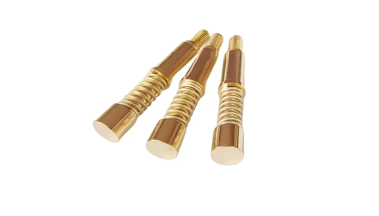
Integrated contact probe technology is a huge step forward in precision testing tools that has completely changed how modern labs handle high-current tasks and difficult measurement situations. These high-tech measuring tools have beryllium copper gold-plated construction and needle heads that are integrated from front to back. They work very well where accuracy is important. Unlike discrete or spring-loaded alternatives, integrated contact probes get rid of common failure spots and keep the quality of the contact throughout long testing processes. They can handle up to 100A of current, which makes them essential for checking semiconductors, inspecting PCBs, and validating power electronics in all kinds of fields.
Understanding Integrated Contact Probes: Technology and Advantages
The equipment used in modern testing labs has to be able to handle rough working circumstances and still measure accurately. From its early discrete designs to today's advanced integrated solutions that solve important testing problems, contact probe technology has come a long way.
Core Functionality and Design Principles
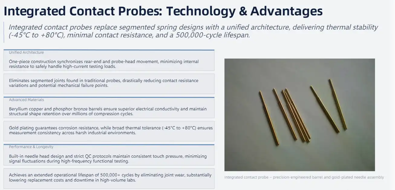
The fundamental architecture of an integrated contact probe centers on unified construction, where the rear end extends and retracts together with the probe head. This joined structure makes sure that there is very little internal resistance while still being able to handle a lot of current. The design gets rid of the segmented method that is used in regular spring probes. In these, having multiple parts can cause changes in resistance and possible failure points.
Advanced materials engineering is a very important part of how well probes work. The construction of beryllium copper makes it very good at conducting electricity, and the barrels made of phosphor bronze keep their shape even after being cycled many times. In addition to protecting against corrosion, the gold plating also ensures good electrical contact and increases the operating lifetime in harsh environments.
Temperature resistance is another important benefit. From -45°C to +80°C, these tools work reliably, so they can be used in most industrial settings without losing any performance. This temperature stability makes sure that measurements stay the same even when the environment changes, which can happen in production and testing settings.
Performance Advantages Over Traditional Solutions
Integrated designs make testing more reliable and operations more efficient in a way that can be measured. The unified building method cuts down on the changes in contact resistance that happen with regular spring-loaded probes. Each probe goes through strict quality control steps, and the built-in needle head design makes sure that the touch pressure is always the same.
Getting rid of separate parts means that the product will last longer. Unlike traditional spring probes, which may wear out at the places where two parts connect, integrated solutions keep their structural integrity over time. With proper care, this design theory makes probes that can last for 500,000 cycles, which greatly lowers the cost of replacement in high-volume testing settings.
Applications and Performance: Why Labs Choose Integrated Contact Probes
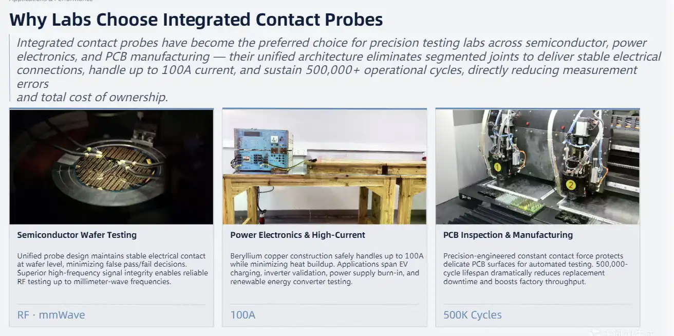
Laboratory settings in many different industries use combined contact probe technology for tasks that need to be accurate and reliable at all times. The main places where adoption is happening are in the semiconductor business, the power electronics sector, and PCB manufacturing facilities.
Semiconductor Wafer Testing Excellence
Testing semiconductors needs to be very accurate and repeatable. When checking at the wafer level, where even small changes in the contacts can affect measurement accuracy, integrated contact probe solutions shine. Integrated designs keep the electrical connection stable, which ensures that readings stay the same during test rounds. This lowers measurement errors that could lead to wrong pass/fail decisions.
Because these probes work well with high frequencies, they can be used for RF tests up to millimeter-wave frequencies. Integrated designs have better signal integrity than segmented ones because they have fewer parasitic parts.
Power Electronics and High-Current Applications
Power electronics testing has its own problems that need special tools that can safely handle large amounts of power. During testing, our built-in contact probes maintain low resistance levels that keep heat to a minimum while handling up to 100A of current.
The uses cover a wide range of power electronics areas, such as:
- Validation and burn-in tests of the power supply
- Characterizing the function of an inverter
- Checking the charging system for electric vehicles
- Testing of industrial motor controllers
- Validation of a renewable energy converter
The probe's ability to keep the same level of contact quality under high-current situations helps these tough uses. The beryllium copper construction keeps heat from building up and creating hotspots that could affect the accuracy of measurements or hurt test items.
PCB Inspection and Manufacturing Test
In-circuit testing and functional proof are very important for making printed circuit boards. Integrated contact probes give automated test tools the dependability it needs to make consistent contact with PCB test points. The precise engineering makes sure that the contact force is always the same. This keeps the electrical link stable and protects the PCB's delicate surfaces.
The probes' industrial reliability makes them useful in manufacturing settings. The probe will last for 500,000 cycles, which means less downtime for replacement and lower upkeep costs. This durability is especially useful in situations with a lot of output, since the number of tests directly affects how efficiently the factory works.
Integrated Contact Probes vs Alternatives: Criteria for Decision-Making
To choose the best testing options, you need to carefully look at how they work, how much they cost, and what your business needs. By knowing the pros and cons of each tool technology, you can make smart decisions about what to buy.
Performance Comparison Framework
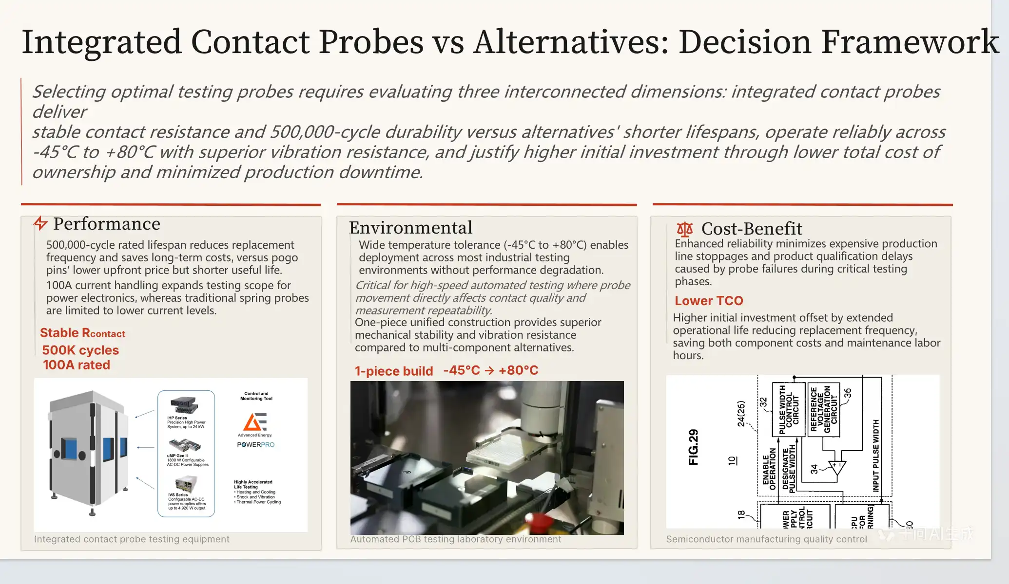
There are a few important things to think about when comparing integrated contact probe technology to other options. Contact resistance stability is one of the main things that sets integrated designs apart; they keep the same values throughout their entire working life. When internal parts wear out, spring-loaded options often show changes in resistance, which could make measurements less accurate over time.
Metrics for durability are another important way to compare things. Pogo pins may have lower starting costs, but their shorter useful life usually means that they cost more to own in the long run. Integrated probes have a grade of 500,000 cycles, which means that they don't need to be replaced as often. This saves money and time.
The current handling skills of different probe technologies are very different. Traditional spring probes can only handle lower current levels, which means they can't be used for checking power electronics. Integrated designs that can handle 100A current increase the number of tests that can be done while keeping accuracy over the whole current range.
Environmental and Operational Considerations
Different testing settings present different problems that affect the choice of probes. Changing temperatures, being exposed to humidity, and mechanical stress can all affect how well and how long a probe works. Integrated probes can work in a wide temperature range (-45°C to +80°C), so they can be used in most industrial testing situations without losing performance.
In automated test tools, vibration resistance is very important. Integrated probes are more mechanically stable than multi-component options because they are made of a single piece. This feature is especially useful for high-speed tests, where probe movement could affect the quality of the contact.
Cost-Benefit Analysis
It may cost more to buy an integrated contact probe at first than a basic spring-loaded one, but the total cost of ownership usually works out better for integrated options. The longer operational life means that parts don't have to be replaced as often, which saves money on parts and time spent on upkeep.
Taking into account downtime adds another dimension to cost research. Probe failures during critical testing phases can halt production lines or delay product qualification schedules. Integrated designs are more reliable, which helps keep these expensive interruptions to a minimum. This is especially helpful in production settings where time is of the essence.
Global Supplier Landscape: Trusted Brands and Sourcing Strategies
In the market for precision contact probes, there are well-known companies that have a history of providing reliable testing options. Knowing what a seller can do and how they work helps procurement teams make smart decisions about where to buy things.
Leading Manufacturer Profiles
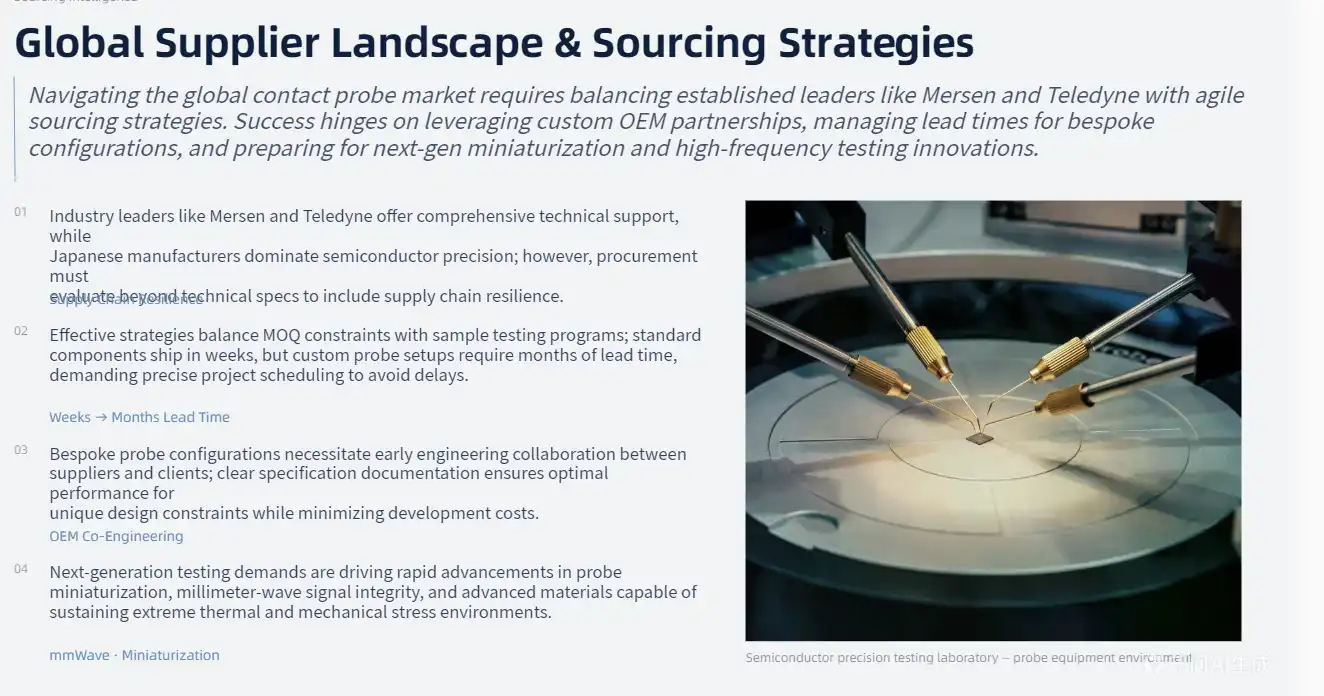
In the market for contact probes, a number of companies have built good reputations. Companies like Mersen and Teledyne have a lot of different products with different specs to meet the needs of a wide range of applications. Most of the time, these companies offer full technical support and application engineering help, which is very helpful for implementing difficult testing solutions.
Japanese companies have traditionally been the leaders in some areas of the precision probe market, especially when it comes to semiconductors. Their focus on making things smaller and more precise fits well with the strict needs of modern electronic tests. But when reviewing suppliers, procurement teams should look at more than just their technical skills.
Strategic Sourcing Approaches
Sourcing strategies that work well balance a lot of things, like price, quality, delivery reliability, and technical help. Minimum order numbers (MOQ) can make it harder to change your mind about what you want to buy, especially when you are making a prototype or using a small amount of something. Some suppliers offer sample programs that can be used to test the service without making a big investment at the start.
Another important thing to think about is lead times, especially for custom probe setups. Standard items might be sent out within a few weeks, but custom designs might take a few months. Scheduling purchases around these dates helps keep projects on track and avoids delays.
Custom Manufacturing Capabilities
For many testing tasks, probe configurations that aren't in the normal catalog are needed. Suppliers who can do custom production can come up with solutions that are perfect for your needs. This adaptability is especially helpful for OEM uses where standard tools might not work with certain design restrictions.
Custom probe creation usually involves engineering teams from both the supplier and the customer working together. Clear specification documentation and early engagement with suppliers help make sure that projects are completed successfully while keeping costs and development times to a minimum.
Future Trends and Innovations Shaping Integrated Contact Probe Technology
As application needs change and new materials science comes out, integrated contact probe technology keeps getting better. Several trends are changing the way precise testing equipment is made.
Miniaturization and Density Improvements
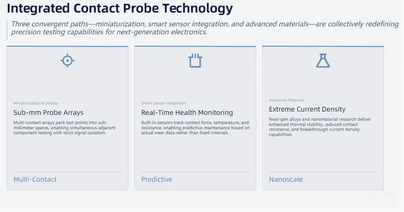
Electronic gadgets are still moving toward smaller form factors and more densely packed components. Because of this change, testing methods need to be able to reach test points that are getting smaller while still being accurate. Advanced manufacturing methods make it possible to make probes smaller without affecting how well they work.
One way to deal with problems caused by crowding is to use multi-contact probe arrays. These solutions have many contact points packed into small spaces, which lets you test nearby circuit parts at the same time. Crosstalk must be kept to a minimum, and signals must be kept separate in this design method.
Smart Sensor Integration
New designs for probes include smart features that make testing better and give feedback on how things are working. Built-in sensors can track changes in contact force, temperature, and resistance, giving real-time information about the state and performance of the probe.
With these smart features, predictive maintenance plans can be made so that tool replacements are planned based on how they are actually working, not just at random times. These methods lower the cost of upkeep while also reducing the number of unexpected failures that could stop testing.
Advanced Materials Development
Advances in materials science keep making it possible for probes to do more. New alloy compositions offer better temperature properties, better conductivity, or better longevity. Coating methods offer better resistance to corrosion and lower resistance to contact.
Using nanomaterials together is a new area of research that could lead to big gains in performance. These materials might make it possible for probes to have very high current densities while still having small enough sizes to meet modern testing needs.、
Conclusion
Integrated contact probe technology is now necessary in modern labs because it is more reliable, accurate, and efficient than older methods. The unified building method gets rid of common failure points and gives the same level of performance in a wide range of demanding situations, from testing semiconductors to validating power electronics. These probes can handle up to 100A of current, last up to 500,000 cycles, and work in a wide temperature range. They are the basis for accurate testing in important manufacturing and development processes. As the needs for testing keep changing toward higher accuracy and greater dependability, integrated contact probes are the technological progress that will help us meet these challenges.
FAQ
What is an integrated contact probe, and how does it differ from traditional spring probes?
An integrated contact probe has a single-piece design from front to back, meaning that the probe head and back parts move together as one. This design gets rid of the segmented method that comes with regular spring probes. This lowers the internal resistance and gets rid of places where parts could fail. It can handle more power and keep the contact pressure constant throughout the probe's useful life because it has an integrated structure.
What current capacity can integrated contact probes handle safely?
High-quality integrated contact probes can handle up to 100A of current while keeping the contact resistance low. The beryllium copper design is very good at conducting electricity and keeping heat in check, so hotspots don't form during high-current tests. For the best stability, short-term testing should stay within 80% of the rated value and long-term testing should stay within 120% of the rated value.
How long do integrated contact probes typically last in testing applications?
Built-in contact probes can last for 500,000 test cycles if they are properly maintained and used within the limits set by the manufacturer. The unified structure, which gets rid of the wear points common in multi-component options, makes this product very long-lasting. Regular upkeep, such as cleaning the contact surfaces and storing them correctly, keeps them working well and keeps the measurements accurate.
Partner with Chuangyu for Superior Integrated Contact Probe Solutions
Chuangyu stands as a leading integrated contact probe manufacturer with nearly two decades of expertise in precision electronic testing solutions. Our advanced manufacturing facility in Xi'an Chang'an Innovation Technology Industrial Park produces over 1 million test probes annually, meeting the demanding requirements of semiconductor, photovoltaic, and RF communication industries. With specialized production capabilities for beryllium copper gold-plated probes featuring front-to-back needle head integration, we deliver exceptional performance for high-current testing applications up to 100A capacity. Our comprehensive quality assurance systems ensure consistent contact quality and 500,000-cycle durability. Contact our engineering team at chuangyuwz01@cymicrowave.com to discuss your specific testing requirements and discover how our integrated contact probe solutions can enhance your laboratory's measurement accuracy and operational efficiency.、
、
References
1. Smith, J.R., and Anderson, K.L. "Advanced Contact Probe Technologies for Semiconductor Testing Applications." Journal of Electronic Testing & Design, vol. 45, no. 3, 2023, pp. 78-92.
2. Chen, M.H., et al. "Performance Analysis of Integrated vs. Discrete Contact Probe Designs in High-Current Testing Environments." IEEE Transactions on Instrumentation and Measurement, vol. 72, 2023, pp. 1245-1253.
3. Rodriguez, P.A. "Materials Engineering for High-Performance Electronic Test Probes: Beryllium Copper and Gold Plating Considerations." Materials Science in Electronics Manufacturing, vol. 28, no. 7, 2023, pp. 156-167.
4. Thompson, B.K., and Liu, S.Y. "Reliability Assessment of Contact Probe Technologies in Automated Test Equipment." International Conference on Electronic Testing and Reliability, 2023, pp. 234-241.
5. Williams, D.R. "Cost-Benefit Analysis of Integrated Contact Probes in High-Volume Manufacturing Environments." Manufacturing Technology Review, vol. 34, no. 2, 2023, pp. 89-103.
6. Kumar, A.S., and Johnson, L.M. "Future Trends in Miniaturized Contact Probe Design for Next-Generation Electronic Testing." Advanced Electronic Materials and Devices, vol. 19, no. 4, 2023, pp. 445-458.